Continue to Site

Eng-Tips is the largest engineering community on the Internet

Intelligent Work Forums for Engineering Professionals

  • Congratulations KootK on being selected by the Eng-Tips community for having the most helpful posts in the forums last week. Way to Go!

ASML's Lithography Plant

Status
Not open for further replies.

Sparweb

Aerospace
May 21, 2003
5,131
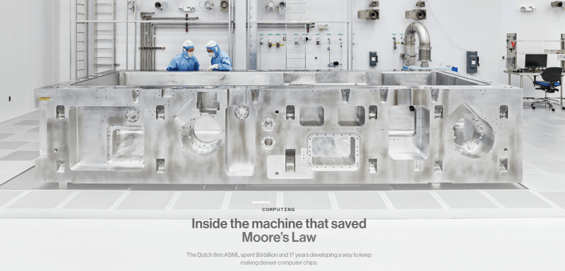
So I've never seen this stuff stripped to the bones, never realized what was hidden inside.

This looks like it was made from a solid block of aluminum 10 meters on two sides, and more than a meter thick. WOW.
The implications to make something like that, and the difficulties that must be overcome, are really hard to think about.
I bet there's a tight tolerance on all of those bolt holes, too.

This photo is from a recent MIT Technology Review article, for those who subscribe: (The comment about Moore's law is just clickbait for nerds like me)
ASML_Microchip_Lithography_Plan_Frame_slp5je.png
 
Replies continue below

Recommended for you

Is this the link to Moore's Law?

Screenshot_2021-11-20_at_08-22-30_Inside_the_machine_that_saved_Moore_s_Law_dv0k3c.png


--------------------
Ohm's law
Not just a good idea;
It's the LAW!
 
Thanks for sharing that Spar. I was able to read some interesting information before the pay-wall cut-off.

--------------------
Ohm's law
Not just a good idea;
It's the LAW!
 
Not just that, but UV lithography had gone from a "1-um is the death of UV lithography" back in the late 70s to going down to 5-nm feature sizes, albeit with double or triple the number of photolithographic masks per physical layer, through people like ASML, Canon, etal. E-beam lithography was going to take over the world in the 80s; just goes to show how hard it is to get people to change the way they do things.

TTFN (ta ta for now)
I can do absolutely anything. I'm an expert! faq731-376 forum1529 Entire Forum list
 
Their EUV stepper is a very impressive and massive machine, I have seen one up close at one of their facilities.
Our company makes the critical nozzle that ejects the tin droplets.

-AK2DM

~~~~~~~~~~~~~~~~~~~~~~~~~~~~~~~~~~
"It's the questions that drive us"
~~~~~~~~~~~~~~~~~~~~~~~~~~~~~~~~~~

 
Sure, somewhat better than the x-ray lithography systems a company across the street tried to develop and sell in 1986, but went bankrupt because the lithography guys refused to leave UV behind.

TTFN (ta ta for now)
I can do absolutely anything. I'm an expert! faq731-376 forum1529 Entire Forum list
 
My company used to supply the high temperature adhesive for the tin nozzle assembly of the EUV Laser. About one drop per nozzle. Not a big seller.
 
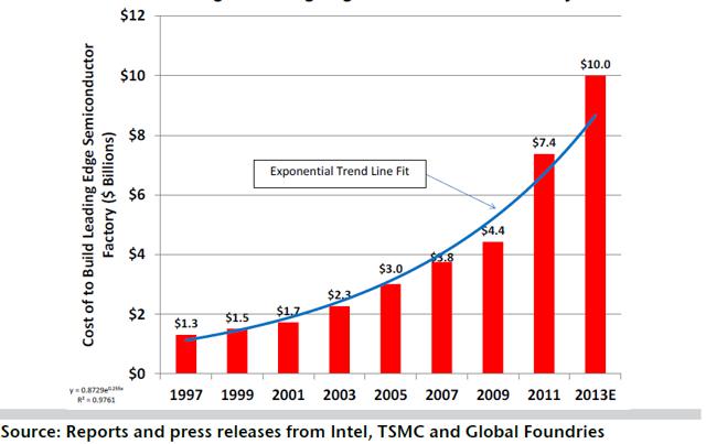
Just for some context, it was reported on Marketplace that Samsung is building a semiconductor plant in the US to the tune of $7B!!!??? WTF? I remember when we thought we could build a small fab for about $40M in 1987.

TTFN (ta ta for now)
I can do absolutely anything. I'm an expert! faq731-376 forum1529 Entire Forum list
 
IR; Look again. You dropped a "1". Please do not set any missile targeting numbers. The plant is going to cost $17B

That's in Taylor Texass (centralish) 30mi from Austin where they have another large fab called Fab1 built in 1996. Samsung is the 2nd largest semiconductor fab company.

Keith Cress
kcress -
 
Status
Not open for further replies.

Part and Inventory Search

Sponsor