Hello!
I've posted this in a wrong group.
Now I'm reposting it here wondering professional answers and suggestions from this group.
Thank you in advance!
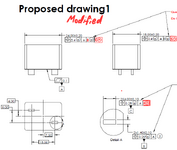
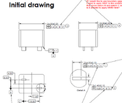
I got confused if the drawing attached is correct or not, actually the 1st drawing was from my customer and probably their drawing follow ISO standard.
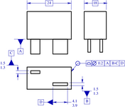
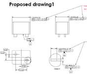
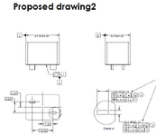
The other 2 proposed drawing are based on my understanding and I think they are clearer and more reasonable.
However I'm a new user of GD&T and I have no confidence of it.
Design intent:
This part is an electronic component with a plastic block and two flat pins(two tabs) protruding the block.
It will be mounted on a PCB with the two pins soldered in PCB holes(slotted hole)
While the pins are in the PCB holes, the upper block are supposed to stay vertical and not shift too much with respect to the pins.
Because if they shift much, the component will take up more room on the PCB and may interfere with adjacent components.
So the design intent is to maintain a good interrelated position among the two pins(taken as a group)
That's why I specify positional tolerance for the two pins as pattern feature.
Also, the upper block need to be constrained by a positional tolerance with respect to the two pins.
Note:
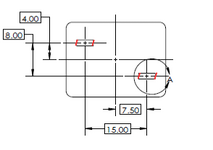
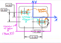
In ASME Y14.5, there are many examples showing hole pattern being used as datum features.
But all of them are round holes.
For this component, there are two flat pins(tabs)
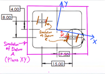
So I have to use two separate datums(datum B, and C) in two directions(X, Y) respectively.
I'm not sure if this drawing indication make sense and if it's measurable with CMM.
For sure it can be inspected using functional gauge with MMC and MMB stated on the drawing.
However, in addition to gauge inspection, we need to get readings for FAI stage and for QA sampling test in production stage.


Attachments
Last edited:


