Continue to Site

Eng-Tips is the largest engineering community on the Internet

Intelligent Work Forums for Engineering Professionals

  • Congratulations Toost on being selected by the Eng-Tips community for having the most helpful posts in the forums last week. Way to Go!

Coplanarity application

Status
Not open for further replies.

SeasonLee

Mechanical
Sep 15, 2008
913
Few questions arose when I saw an IC package outline drawing last week, pls ref to the attached for details, my questions:

Question 1: Can we delete the datum reference C from profile FCF?
Question 2: Profile tolerance value will be less than the size tolerance, am I right?

Thanks for your valuable comments.

Season


 http://files.engineering.com/getfile.aspx?folder=657a0852-5e34-4377-a94d-551488486bed&file=IC_lead_package_dim_Questions.pdf
Replies continue below

Recommended for you

Lots of issues on that print...

Datum feature C isn't labeled; that's the first problem. But assuming it's the main flat face, then it's OK to leave datum C reference in the profile callout.

Since that profile is 2X, the profile itself controls the size (height and width), so there is no reason to have the profile be less than the size tolerance (the size is basic).

Several other things (such as the composite position being changed to 2 single segments with 2 position symbols), but I hope that helps for your original questions.

ADDED TEXT: see next post

John-Paul Belanger
 
My bad -- I just now scrolled to the second page. So yes, datum C is fine. But the profile tolerance value might still be OK, because the dimension of 0.00 to 0.05 looks to be tagged to a different level. And it's not really a feature of size, so there's no Rule #1.

John-Paul Belanger
Certified Sr. GD&T Professional
Geometric Learning Systems
 
I agree with John-Pauls' assessment. Did I miss something - what dimensions controls the distance from "Datum C" face "up" to the 48 coplaner surfaces?

Certified Sr. GD&T Professional
 
Thanks for your comments, JP.

There are 3 pages on my attachment, page 3 mentioned the coplanar surface is composed of 64 lead surfaces and the exposed die pad, a profile control will be used to treat them as a single surface, in this type of application, the profile control is a form control and does not use datum references, example is shown below. I still can’t understand “datum C is fine” here, would you please have more detailed interpretation on it.
2016-11-08_034513_riafqe.jpg


Season
 
I would aldo replace profile to C in the main view with perpendicularity to C for datum feature A side and with perpendicularity to C primary and A secondary for datum feature B side.
 
Yes, SeasonLee, your proposed change makes MUCH more sense. The original use of a phantom line didn't really make sense, since there is no nominal around which to make it unilateral. I guess that's why I didn't even understand what was being pointed to.

Your second question seems to bring up a good point too. If the profile tolerance is really utilized to that full 0.08, it will make some of the surfaces sit below the other surfaces, which is exactly what you don't want. Sure, you can make the profile tolerance less than 0.05, but make sure that they can still hold that.

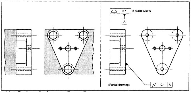
Greenimi -- What you suggest wouldn't be the same thing. The current use of profile on those 4 edges (2X for each profile) controls the form, orientation, location, and size of the full perimeter. It's essentially an "all around" profile (which would have been an easier way to show it).
Perpendicularity would only control form and orientation, and require the basic dims to be changed to toleranced dims.

John-Paul Belanger
Certified Sr. GD&T Professional
Geometric Learning Systems
 
I feel like the relationship between C versus A and C versus A and B is orientation only. In the shown configuration, C being primary then the secondary is to be oriented to C and not located.

I would say if you cannot say for sure/ you cannot tell how far apart is C from A and/or from B respectively, then the correct callout is orientation and not location. Same design intent, but bad “grammar” in GDT language.
 
JP, Thanks for your inputs again. If I were the designer I will delete the datum reference C from profile FCF, and reduce the profile tolerance value to 0.05 at least in this particular case, the revised sketch looks like it below.
2016-11-09_002813_d0xetd.jpg


John-Paul Belanger said:
Several other things (such as the composite position being changed to 2 single segments with 2 position symbols)
May I ask why will you make the change from composite position to two single-segment position callout? I don't want anything missed on this thread.

Season
 
I have been following this thread. I have ask, was any consideration given designating the "top" surface as Datum C and have the tips of the (48) pins individually profile-controlled "parallel" to the top. This would eliminate the need to use the coplanar control.

Certified Sr. GD&T Professional
 
Greenimi, I presume you're talking about the first picture in that 3-page drawing. In that case, the profile tolerances fall under the rule of "simultaneous requirements." (Paragraph 4.19 of Y14.5)

So the four sides are not just oriented, but also distanced apart. IOW, the max width of the square is 7.1 mm, and the min could be 6.9 mm.

John-Paul Belanger
Certified Sr. GD&T Professional
Geometric Learning Systems
 
John-Paul:

Regarding your statement "The current use of profile on those 4 edges (2X for each profile) controls the form, orientation, location, and size of the full perimeter. It's essentially an "all around" profile (which would have been an easier way to show it)." I think using 2X to cause the profile to apply to the opposite surface is a push. I cannot understand how you get to the "all around" interpretation. Can you expand on this?

Certified Sr. GD&T Professional
 
Not part of the OP's original two questions but the top line of the composite profile (PLTZF) needs to be changed to C then A then B for the second line to be meaningful.
 
mkcski,

I can only turn the question around to you, and ask what the 2X could possibly mean to you if it's not referring to the opposing side?

(The all-around idea comes from the additional fact that these are simultaneous requirements.)

John-Paul Belanger
Certified Sr. GD&T Professional
Geometric Learning Systems
 
mkcski

2X on two sides means all around, I believe it's a bad “grammar” in GDT language(quoted from greenimi), pls see the figure below, you may find it out at page 25 on this document, “IC Packages / PCB Footprint Guidelines”, just google it.
2016-11-09_111551_a8rsod.jpg


Season
 
SeasonLee:

Thanks for responding. I am not familiar with PCB industry product definition drawings so your all around interpretation is not on my "list". Additionally, Y14.5 is for "engineering drawings" and I work with large machinery, so I use "mechanical" eyes when review drawings. If you look a the list of companies that Y14.5 Committee members work for, most make "mechanical" products, so the examples in the Y14.5 are predominately mechanical parts. So, is a PC board an engineered part - I think it is. Maybe PC companies should lobby for examples of PC boards in the Y14.5 standard.

You can be "creative" and use "bad grammar" but you run the risk of miscommunication. I also recognize Y14.5 does not show every possible application (considering what I said earlier). Consequently, many industries use GDT in "special ways" and this gets propagated by documents like you referenced. In my mind, this doesn't justify "bad grammar" but should encourage readers/users to present challenges to the governing body of the document - the Y14.5 Committee is sanctioned by ASME - to make changes at the next issue of the document or release errata revisions every so often. Is the document you referenced sanctioned our just something that has evolved and that everyone "trusts" for guidance? I do not have time right now to find and reviews the "IC Packages / PCB Footprint Guidelines” you mentioned. Food for thought.

Certified Sr. GD&T Professional
 
SeasonLee:

I had a chance to google the phrase and found the underlying document is not an PCB industry standard that is sanctioned by a governing body, but is an internal "standards" document for TRINAMIC Motion Control GmbH & Co. So I ask: unless you work for them, why do you use this as an trusted "dictionary"? I also note that the 2X for profile was not shown anywhere and that the "as per Y14.5" all-around "circle" was used in many examples to define part exterior geometry (as you posted earlier).

I may be beating a dead horse, but I still cannot get to "all around" interpretation per 4.19 SIMULTANEOUS REQUIREMENTS using the 2X notation in your OP. I cannot connect the 2 pairs of sides using the understood BASIC 90-deg (at the corners) to control the orientation (perpendicularity) relationship between the 2 pairs to create a BASIC square "pattern". If you had one profile-of-a-surface FCF with 4X I could see the four sides being connected as one square festure, but the 2X doesn't' get me there.

I really appreciate your post for exposing me to the use of GDT for the PCB's.

Certified Sr. GD&T Professional
 
'All Around' is a general shortcut for any number of individual callouts that would define the perimeter. There isn't anything that one needs to 'get to.' The only reason 'all around' would be a substitute for this case is that there is an equivalent value for the tolerance. It is possible that each pair of faces would have a different value and therefore 'all around' would not be used.

Look what happens when the first part of the 'or' clause is removed:

4.19 A simultaneous requirement is where two or more geometric tolerances apply as a single ... part requirement.
 
3DDave:

After following this thread, I better understand that 2X with identical datum sequences means "all around". I guess my "limited" exposure to the application and interpretation of profile as related to 4.19 Simultaneous Requirement prevents me from an "instantaneous" understanding. Being confused, I have go to square-one: review the basic GDT conventions and apply them to one-by-one to the dimension schema to say "ah, that means all around". Thanks for showing me the way.

Certified Sr. GD&T Professional
 
Status
Not open for further replies.

Part and Inventory Search

Sponsor