Eng-Tips is the largest engineering community on the Internet

Intelligent Work Forums for Engineering Professionals

  • Congratulations waross on being selected by the Tek-Tips community for having the most helpful posts in the forums last week. Way to Go!

Need Help Identifying PCB Design Feature

Status
Not open for further replies.

Travman1023

Mechanical
Apr 10, 2014
3
0
0
US
Hello,

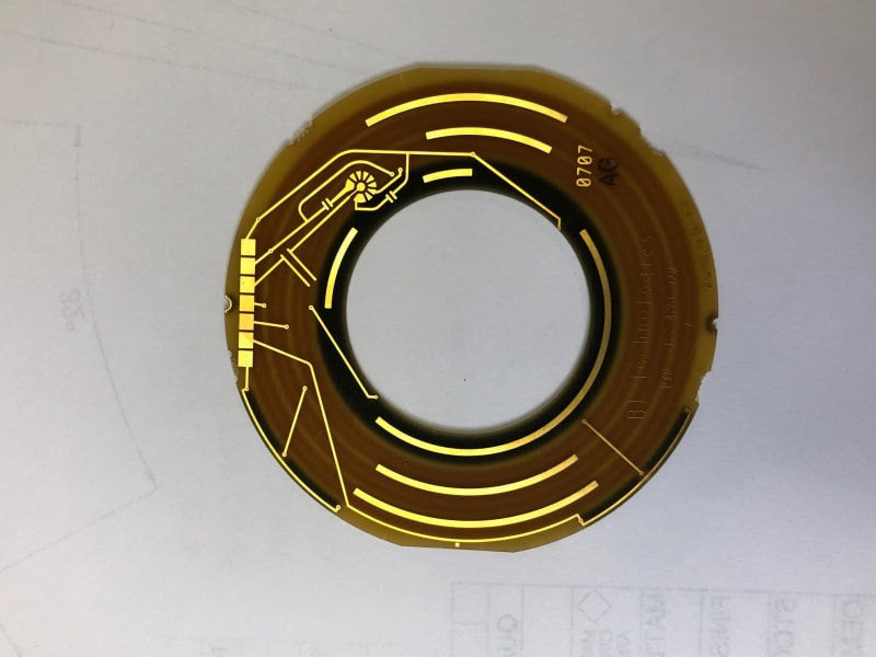
I am looking at a steering angle sensor that has a printed circuit board with this wheel-shaped array of copper pads (see image). I am trying to get more info on how and why it works, but I don't know what this thing is called. Is it a capacitor? A switch? Or is it for a coil inductor? There wasn't any components or parts above it so I am thinking it might be for a different application or obsolete tech. I am an ME so my EE knowledge is limited. Thanks for any tips or feedback!
Position_PCB_-_Back_-_COIL_INDUCTANCE_ANTENNAE_SWITCH_lc5x9p.jpg
 
Replies continue below

Recommended for you

I'm guessing that it is a schematic diagram of the printed circuit. There is no added cost to doing it this way since the circuit itself must be printed.
 
Normally I would say it's a rotary encoder or multi-position rotary switch (one connection at center spoke, second connection to multiple possible paths, 2/3rds of which don't connect to anything), but the schematic-looking capacitor marks have me seriously scratching me head. Can we see an overall pic of the entire board (and maybe something in the pic for scale, like a quarter or a ruler)?

Dan - Owner
Footwell%20Animation%20Tiny.gif
 
Position_PCB_-_Back1_ljrmrh.jpg


there is the backside.

I.D. of PCB is 1.5in
O.D. of PCB is 3.0in

most right pad (#1) is Vcc 5.0V
Pad #2 is GND

thank you for the comments/direction

-T
 
Just a guess. It looks like the encoder is based on a capacitance sensing method. There are four outer tracks of encoding plus one inner track of (possible) zero index. It looks like the PCB feature circles on an area where there are no tracks. So my guess would be that this PCB feature is a reference capacitance to determine the gap to the metal index ring to get additional accuracy for the encoding. The capacitor symbol-like traces may be there to determine the PCB dielectric constant for calibration/test of stuffed PCB before final assembly as an encoder. With a stuffed PCB w/o encoder ring calibration they can adjust for variations in the PCB dielectric constant variations lot-to-lot. And if they're really clever, the PCB feature can also help compensate for the capacitance change in the field as the PCB moisture content varies due to seasons, temperature, or relative humidity.
 
Status
Not open for further replies.
Back
Top