Continue to Site

Eng-Tips is the largest engineering community on the Internet

Intelligent Work Forums for Engineering Professionals

  • Congratulations SE2607 on being selected by the Eng-Tips community for having the most helpful posts in the forums last week. Way to Go!

Stress on HV Insulators 1

Status
Not open for further replies.

basilasq1

Electrical
Jun 11, 2014
18
Hi Everyone,

Our utility clients usually specify a minimum phase to ground clearances for high voltage (>69kV) substations. While we always meet those requirements, what potential issues would you all see in the following arrangement:

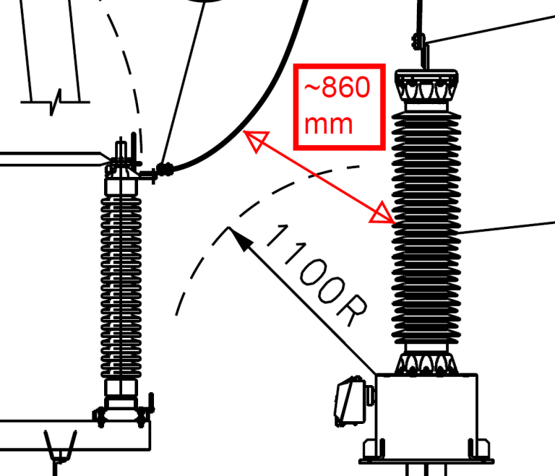
A live wire jumper is connected in such a way that it meets the min. clearance to ground for the grounded parts of the HV equipment (CVT) but is much closer to the middle of the CVT insulator (min ph-ground clearance is considered as 1100mm for 138kV system). Refer to the following pic for details:
CVT_clearance_z3hcpg.png


My questions are:
Will this increase stresses on the insulator and degrade long-term performance?
Will the problem be exacerbated for higher voltage levels (240, 345kV)?

Thanks for you feedback.
 
Replies continue below

Recommended for you

The top part of the insulation is also that close to the energized conductor on top of itself and is designed to be that way with no adverse effects.
 
It may or may not create problem. It will not degrade insulator but can cause a flashover or failure of CVT.It depends what is the potential level at CVT where the minimum clearance occurs. It will not be earth but anything between 0-100 % of line potential.
 
Is this drawn to scale? If I put a straight line from energized cap of the insulator to the energized top of the CVT, the conductor does not appear to drop below it. Draw another line for ground potential plus a few more to represent lines of equal potential to represent the gradient and you should see evenly spaced parallel lines. If the conductor intruded into this area, the gradient would be altered.
 
CCVT_Clearance_ylcgwm.gif


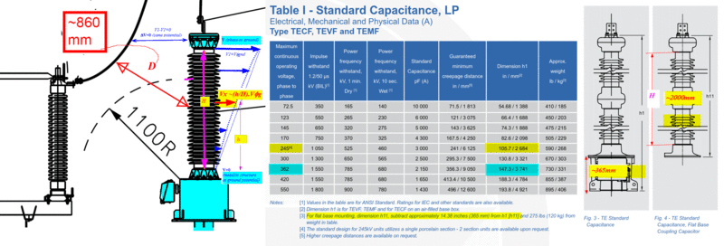
Considering that the voltage difference varies from phase-to-ground voltage on top of the CCVT to 0 at the bottom of the metallic base, the clearances between the conductors could be estimated as the difference between the conductor voltage phase to ground to the voltage at specific point of the CCVT insulator. This voltage difference drives the minimum phase to ground clearance as shown in the enclosed sketch.
For application at voltage higher than the 230 kV, the clearances should be based in the switching surge factor associated with the BSL rather than the BIL. Smaller clearances thank phase to ground could be allow if the insulation coordination between the CVT and the phase conductor is followed.

For porcelain insulator a flashover could be considered as a self-restore event and the risk to damage or degrade the insulator is small. For CVT with polymer insulator the situation is more delicate.
 
Thanks a bunch for everyone's response.

@cuky2000
Your reply does make sense. Is there a simulation program that can be used to estimate the potential at each point on the insulator? My guess is that the potential drop would not be linear through the surface of the CVT insulator.


I assume you're speaking to the voltage gradient down the insulation from line to ground potential.

A CVT is going to have an almost perfectly linear voltage gradient. So, for example, at the mid-point of the insulator, you can assume the voltage to be about 50% of the line-to-ground voltage.

Just giving it the eye-ball test, I would say that the dimensions you listed above would not pose a problem. But, keep in mind, for a CVT, the problem would not be insulation performance alone, but also the potential impact on accuracy performance of the CVT. Influencing the voltage gradient and/or introducing excessive additional stray capacitance can certainly impact the CVT's accuracy.
 
Great point @scottf about stray capacitances. I will keep those requirements in mind.

 
Status
Not open for further replies.

Part and Inventory Search

Sponsor