Ramblin_Man
Mechanical
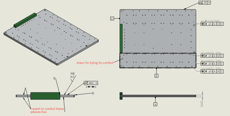
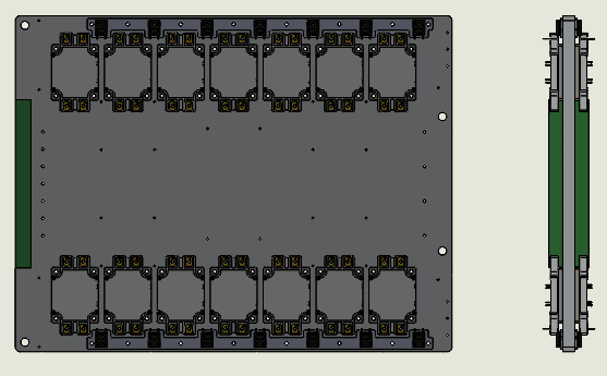
I'm designing a coldplate to mount IGBTs to. The IGBT manufacturer specifies a certain surface finish and "warpage" for the plate, 100um per 100mm. I'm assuming warpage is waviness (mfg is Japanese). I'm also assuming warpage is equivalent to flatness per area, which is how I'm trying to call it out.
I don't need the whole plate to meet this spec, just the areas that IGBTs will mount to. I've tried my best to call this out with GD&T per ASME standard but I'm not sure that its correct. They give no example of controlling a rectangular area of a surface, just a surface between two datum points. Also I have no idea how to apply surface finish to just a certain area of a surface, I see no example of attaching a surface finish callout to a GD&T callout like you do with say hole sizes. And then do that for three more areas without 6 extra datum. Drawing is attached. Thanks

I don't need the whole plate to meet this spec, just the areas that IGBTs will mount to. I've tried my best to call this out with GD&T per ASME standard but I'm not sure that its correct. They give no example of controlling a rectangular area of a surface, just a surface between two datum points. Also I have no idea how to apply surface finish to just a certain area of a surface, I see no example of attaching a surface finish callout to a GD&T callout like you do with say hole sizes. And then do that for three more areas without 6 extra datum. Drawing is attached. Thanks


