Jdo300
Electrical
- Feb 21, 2005
- 6
Hello,
I am working on the design of a flyback converter based on the LT3751 capacitor charging circuit. My design is similar to the 42 A cap charger example on pg. 25 of the LT3751 datasheet. In my case, the circuit runs on 12V and steps up the output to 430 V, but I am having some major noise issues with the MOSFET driving the primary of the transformer. The flyback powers some other high voltage circuitry and the noise from the FET during turn-off is radiating into the other parts of the design, both through the power and ground lines and through the air.
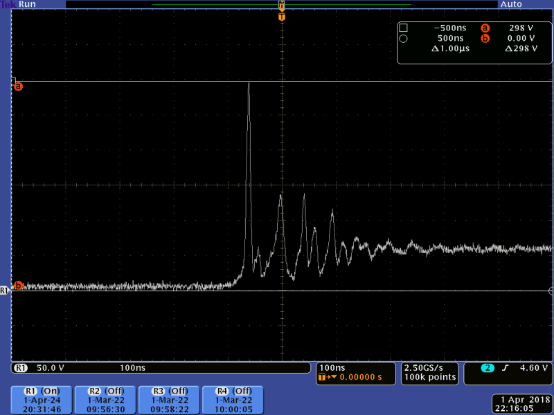
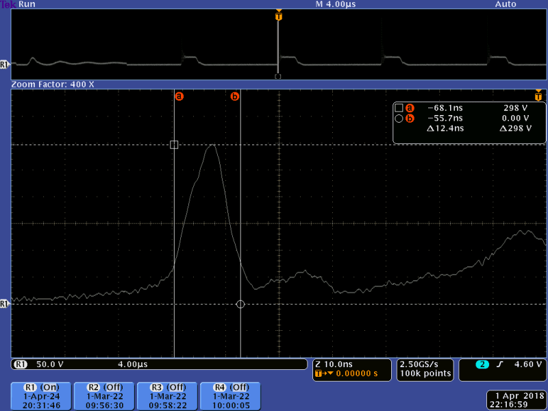
My first attack plan was to add an RC/RCD snubber across the primary of the transformer to snub the high frequency oscillations on the switch. But for some reason, none of the values I calculated for it, (or just plan experimented with) had any real impact on the waveform -- in particular, the first high voltage spike, which is rising to as high as 200 V. I have attached scope shots of the turn-off waveform, including a closeup of the first spike, which is around 12 ns wide. One challenge is that this waveform's spike is so narrow, and also the waveform seems to be rich in harmonics.
Has anyone run into problems like this before or seen a waveform such as this which seems to defy normal RC/RCD snubbers? I'm not sure what to try next to remove this noise.
MOSFET Drain turn-off Waveform

MOSFET Drain turn-off Waveform (Closeup)

- Jason O
I am working on the design of a flyback converter based on the LT3751 capacitor charging circuit. My design is similar to the 42 A cap charger example on pg. 25 of the LT3751 datasheet. In my case, the circuit runs on 12V and steps up the output to 430 V, but I am having some major noise issues with the MOSFET driving the primary of the transformer. The flyback powers some other high voltage circuitry and the noise from the FET during turn-off is radiating into the other parts of the design, both through the power and ground lines and through the air.
My first attack plan was to add an RC/RCD snubber across the primary of the transformer to snub the high frequency oscillations on the switch. But for some reason, none of the values I calculated for it, (or just plan experimented with) had any real impact on the waveform -- in particular, the first high voltage spike, which is rising to as high as 200 V. I have attached scope shots of the turn-off waveform, including a closeup of the first spike, which is around 12 ns wide. One challenge is that this waveform's spike is so narrow, and also the waveform seems to be rich in harmonics.
Has anyone run into problems like this before or seen a waveform such as this which seems to defy normal RC/RCD snubbers? I'm not sure what to try next to remove this noise.
MOSFET Drain turn-off Waveform

MOSFET Drain turn-off Waveform (Closeup)

- Jason O
