Continue to Site

Eng-Tips is the largest engineering community on the Internet

Intelligent Work Forums for Engineering Professionals

  • Congratulations cowski on being selected by the Eng-Tips community for having the most helpful posts in the forums last week. Way to Go!

GD&T question 5

Status
Not open for further replies.

lwh723

Mechanical
Mar 1, 2016
4
Hi,

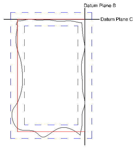
So hoping some experts can help me put a question to bed. I work in the electronics industry, so really don't need to use GD&T at all. However, our data sheet drawing has this call out, and it's been the source of much debate with some customers. I've attached a picture of how I understand it, but some customers are taking it to mean that the 0.1 profile zone encompasses the B & C edges of the part. But those are datums, so shouldn't be included, right? In general, I think it's just a poorly done, but that's another issue.

 
 http://files.engineering.com/getfile.aspx?folder=d2f42e22-e671-4c63-8243-8678066fd906&file=drawing.pdf
Replies continue below

Recommended for you

B & C are the datum planes which are derived by the three highest points on their respective surfaces, which are subject to the profile tolerance in your drawing (since "all around" is specified).

"Know the rules well, so you can break them effectively."
-Dalai Lama XIV
 
Also, the profile callout does not constrain the thickness of the plate. Just labeling a surface as "Datum A" does not control anything about it.
 
B and C datum planes are not edges, but center-planes derived from dimensions 4.9 and 8.2. It is "poorly done", but all 4 edges must be controlled.

0.8 MAX is not a tolerance, because it is one-sided. Flatness of 0.1 controls the surface of datum feature A.

Unless something else is controlled wrt A|B|C, you may be able to drop B and C altogether.

"For every expert there is an equal and opposite expert"
Arthur C. Clarke Profiles of the future

 
I misread the symbol placement; CH is correct and makes a valid point about the necessity of B & C.

"Know the rules well, so you can break them effectively."
-Dalai Lama XIV
 
lwh723 said:
...but some customers are taking it to mean that the 0.1 profile zone encompasses the B & C edges of the part.
they are correct. The profile zone encompasses all 4 sides. Datums B & C are shown as centerplane datums and are not the edges of the part, I agree they are not needed.

lightweight, cheap, strong... pick 2
 
Thanks guys. Looks like I'm going to have to eat a little crow on this one. :)
 
I worked in the electronics industry for 8 or 9 years working as a mech. designer, and I can tell you that GD&T is just as helpful there as it was working for a firearms manufacturer. Anytime you have a physical part, and you want to control is size/shape/orientation, you should probably be using GD&T. Are you making PCB's? Do they have holes required for assembly? I worked on making hermetic enclosures for multi-board signal filters. GD&T was necessary. The main idea as I understand it though, is to control your functional surfaces and the position of functional features of size with GD&T. Perhaps profile of a surface on a PCB is overkill, as the sides of the part are not functional, but it all depends on the application, where it's going and how it's manufactured.
 
lwh723,

Sorry to complicate this, but your drawing happens to include a couple of subtleties (oddities?) of the Y14.5 standard.

First, I would say that B and C are not centerplane datums. Datum feature B is just the right-hand surface and datum feature C is just the top surface. The 4.9 and 8.2 widths are not considered features of size, because the dimensions are basic. If the 4.9 and 8.2 were not basic and had direct plus/minus tolerances, then the widths would be considered features of size and the B and C datums would be centerplanes.

Second, I would agree that the profile tolerance includes all 4 sides. But there is a quirk because the datum features are included. Because datum planes B and C are derived from the high points of the B and C features, the effect is that only half of the profile zone is usable. So the B and C surfaces must be flat within 0.05. Something like this:

AllAroundProfileIncBC_yoov7m.png


Evan Janeshewski

Axymetrix Quality Engineering Inc.
 
axym,

ASME Y14.5-2009 para. 4.11.4 (Specifying Datum Features RMB) does not mention features of size. Where is this requirement for centerplane datums?

- pylfrm
 
pylfrm said:
ASME Y14.5-2009 para. 4.11.4 (Specifying Datum Features RMB) does not mention features of size. Where is this requirement for centerplane datums?

Not only there is no requirement for feature of size, the dimension line itself doesn't even have to contain actual dimension.

"For every expert there is an equal and opposite expert"
Arthur C. Clarke Profiles of the future

 
This specific example could eliminate B and C from the FCF and not be changed.
 
Agree that B&C datums aren't needed for this view, but they are used for the bottom side of the part to control ball grid array locations relative to package edge.

What we ended up doing was leaving datums in place for BGA location, but changing the package size dimensions to 4.9 +/-0.05 and 8.2+/-0.05.
 
axym said:
Sorry to complicate this, but your drawing happens to include a couple of subtleties (oddities?) of the Y14.5 standard.

First, I would say that B and C are not centerplane datums.
this is incorrect. The OPs attachment clearly shows B & C as centerplane datums per ASME Y14.5 when the datum symbol is placed in line with the feature of size it is a centerplane datum. See ASME Y14.5-2009 fig 3-4.


the result of the OPs drawing is a 0.1 profile of all 4 sides.

lightweight, cheap, strong... pick 2
 
They are not needed in the FCF - Feature Control Frame.

I guess you eliminated the profile tolerance? This leaves the orientation of sides to ends at the mercy of the default angle tolerance, if there is one.
 
Hi All,

I expected some disagreement regarding the centerplane datums for the basic widths.

pylfrm - I agree that 4.11.4 does not specifically mention features of size. But it makes no mention of a basic size either. In the figures that show a dimension for a width datum feature, the dimension is always directly toleranced. I was not able to find an example that uses a basic width (or a basic diameter, for a cylindrical datum feature).

CH - There are some figures in section 4 on width datum features, that only show a datum feature symbol and a dimension line (no dimension is shown). Does this mean that this is a legitimate way of specifying a datum feature? I would say no, because these figures are intentionally incomplete.

Tenkan - I agree that the placement of the datum feature symbol and dimension line makes a difference with width datum features of size. But because basic dimensions were used, I would argue that the 4.9 and 8.2 widths are not features of size. The definition of a regular feature of size in 1.3.32.2 contains the statement "associated with a directly toleranced dimension". I would say that a basic width controlled by a profile tolerance is not a directly toleranced dimension - you (and others) may disagree.

So at the end of the day, Y14.5 does not give a clear indication of whether or not a basic width results in a centerplane datum. It makes no indication that you can do this, but doesn't say that you can't. So we have to decide whether this is a valid extension of principle. Overall, I would say that it is not.

Evan Janeshewski

Axymetrix Quality Engineering Inc.
 
Evan, just to keep the pot stirred, here's an offshoot question based on your earlier sketch...

If it's true that only half the tolerance zone is usable on that side, then I'd like your views on what the tolerance zones would look like for each part in my attached graphic. (I'm not interested in whether we all like the second picture; but interested in how folks would envision the tolerance zone if that's what the drawing showed.)

PS: (a corrected graphic is given in a subsequent post)

John-Paul Belanger
Certified Sr. GD&T Professional
 
 http://files.engineering.com/getfile.aspx?folder=6d61caea-cb0a-470a-ad97-3d10c321ba4a&file=Coplanars.jpg
JP,

Hopefully I can offer an opinion here as well. In the first picture I would envision a tolerance zone that extends from the high points of the surface, up 1mm, just like shown in the standard (I think). As for the second picture, I think it would be sheer guesswork. What is datum feature A exactly? According to the print it's the surface on the left only, but then both surfaces are referenced WRT to datum A so that makes it kind of a self referencing datum which is no good. I can't imagine a valid, or at least supported, tolerance zone setup for this.

John Acosta, GDTP Senior Level
Manufacturing Engineering Tech
 
Doh -- yes, I goofed on the picture John. Thanks for pointing that out.

See one version of a corrected graphic (attached). But you might see where I'm going with this: Most of us acknowledge that the first picture places the tolerance zone all on the "up" side. I wonder if people would think the same on the second picture I give?

John-Paul Belanger
Certified Sr. GD&T Professional
Geometric Learning Systems
 
 http://files.engineering.com/getfile.aspx?folder=854e89c6-d079-4fb1-b093-24ba81b9d43d&file=Coplanars1.jpg
Evan,
You may want to take a look at fig. 4-33. This figure does not seem to support your standpoint.

Besides, if we really want to analyze the paragraphs in the standard, para. 3.3.2(b) states that datum is a center plane if the datum feature symbol is placed on the dimension line or an extension of the dimension line of a feature of size. It does not say 'regular feature of size'. The widths in question are features of size, just not regular, but irregular, as defined in para. 1.3.32.2(a).

J-P,
On your first picture the maximum possible offset between both surfaces can be 1. On the second picture only 0.5, because half of the tolerance zone width is unsable as it lies inside the material of datum feature A-B simulator, and the datum A-B is established by the high points of surfaces A and B simultenously.

This concept has not been explicitly pictured and described in the Y14.5-2009, but most likely will be covered in the future version of the Y14.5. From existing standards the closest is fig. 4-16 from Y14.8-2009. It shows datum target application, but the basic tenet is the same - profile tolerance zone applied to datum features from which datum plane is derived is equally disposed about that datum plane. This means that in case of datum targets the entire profile tolerance zone is usable, but in case of datum feature being entire surface only half of the profile tolerance zone is usable.

3DDave,
With that being said, in the OP example there would be a difference between having and not having datum feature reference B and C in the profile callout. Since only half of the profile tolerance zones are usable for each pair of opposed surfaces when B and C are referenced, the maximum allowed angular error between surfaces in each pair (expressed in linear units) is twice as small as in case of profile callout with no datum references or reference to A only. I am not saying that presence of B and C makes sense from functional point of view, just trying to describe difference.

Hope this helps.
 
Status
Not open for further replies.

Part and Inventory Search

Sponsor