Eng-Tips is the largest engineering community on the Internet

Intelligent Work Forums for Engineering Professionals

Traxxas Charger Blown Up.

Status
Not open for further replies.

Sam Neall

Mechanical
Mar 26, 2020
32
0
0
US
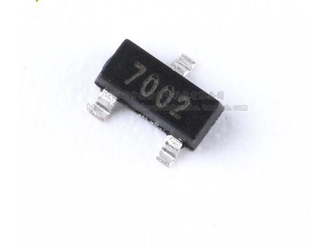
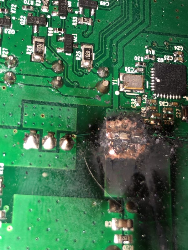
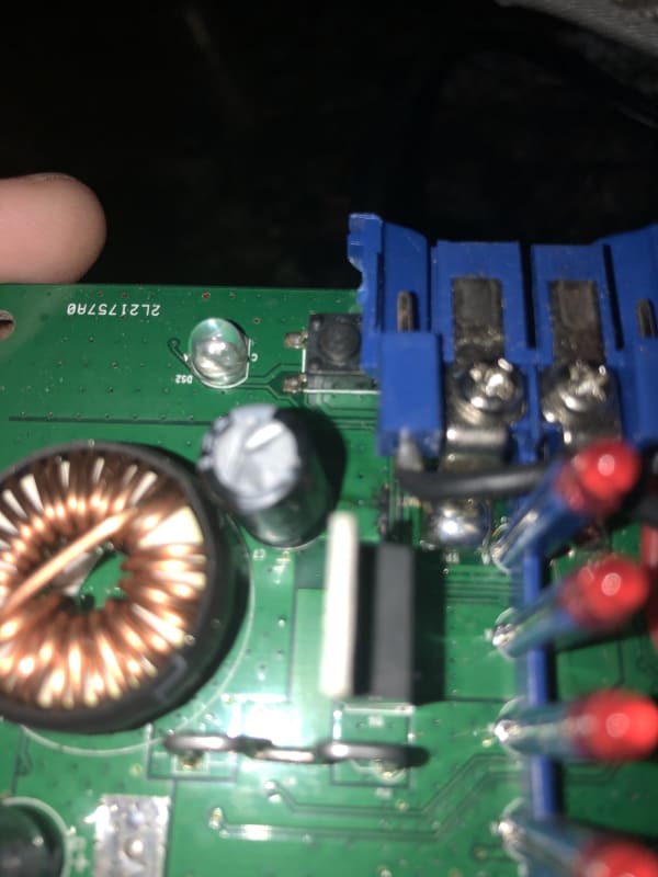
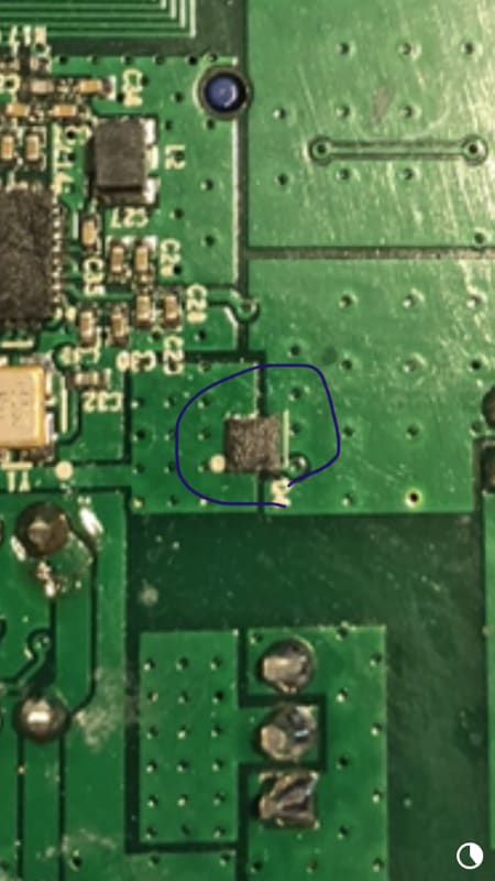
Some factory worker wired my charging adapter backwards so it blew up my charger when I tried to plug the battery in. I’d like to see if I can fix it because this charger is discontinued by its manufacturer. The part that blew out looks to be a SMD resistor, but I’m not sure. I think the heat loosened up some of the outer layer of the board so when I scraped it away with a screwdriver, the copper pads got exposed. What is this component, and is it practical to repair?
image_eqldzl.jpg
 
Replies continue below

Recommended for you

That does NOT look like it was a resistor. I'd guess it was a MOSFET and it certainly toasted.

It will be very hard to guess what that was.. I'd say replace it with another UL listed charger so the place doesn't burn down some night.

Otherwise I'd try to find another unit so you have something to look at so you can determine what that IC was.

Keith Cress
kcress -
 
Hard to tell whether it was a transistor or not. The truckload of vias suggest extremely high currents. However, it has some visual similarities to the component on the left, which looks possibly to be a BJT wired like a diode, which is weird.

A picture of the other side of the board might be more useful

TTFN (ta ta for now)
I can do absolutely anything. I'm an expert! faq731-376 forum1529 Entire Forum list
 
The other side of the board is just green PCB. It’s not a through hole component. You can see the burn mark to the right of the capacitor.
image_z48evn.jpg
 
With the big inductor (circle thing) right next to it on the bottom I'm thinking it might have been a voltage/current regulator before the magic smoke leaked out. What model charger was this?

Z
 
The component circles in blue in the last image is likely a FET. Notice the single via to the lower right that's separated from the copper fill? That's likely to the gate pin, and the two copper fills on either side are the drain/source pins.

Of course it could also just be a large 0-ohm jumper resistor... difficult to be sure with out of focus pics and no way to rotate the board plane to see around the component [wink]

Dan - Owner
Footwell%20Animation%20Tiny.gif
 
Unforunately, the blue marking also obscures the silk-screened component designator; it looks like either Q4 or D4. A better picture of the designator would still be useful

Note that the other transistors in the area appear to be 2N7002 gullwing devices.

AJWY_1_201907251227081936.jpg


TTFN (ta ta for now)
I can do absolutely anything. I'm an expert! faq731-376 forum1529 Entire Forum list
 
I believe it's D4. Note the BAR on the right and the dot. On the cooked board I'm betting the current went crazy for whatever reason and the diode drop dished up all the power dissipation. I'm thinking Dan's via is just a weird thermal as they're all over the place in their looks.

Granted the photo leaves a lot to be desired. It doesn't even give a lot of the board for style comparisons.

Keith Cress
kcress -
 
Status
Not open for further replies.
Back
Top