Eng-Tips is the largest engineering community on the Internet

Intelligent Work Forums for Engineering Professionals

Datum selection and dimensioning - quadruple saddle clamp 2

Status
Not open for further replies.

itar

Aerospace
Jun 11, 2024
4
0
0
CA
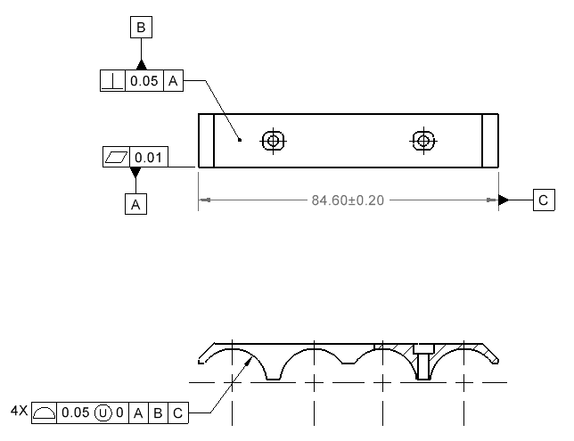
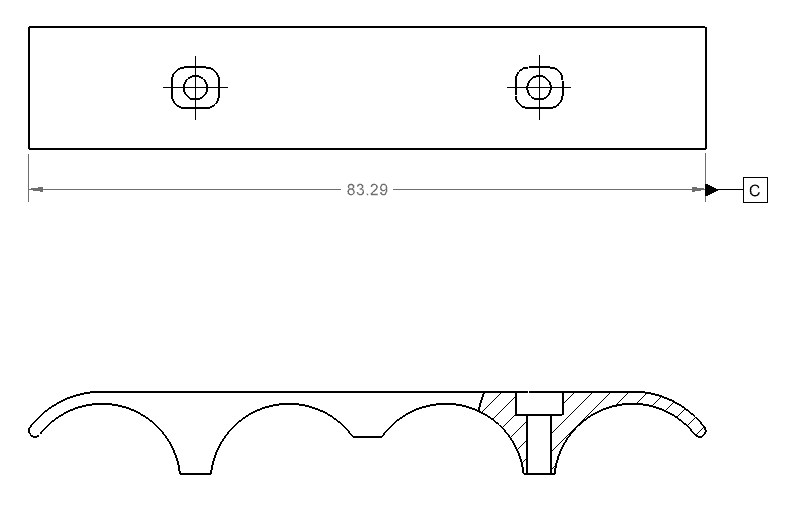
I have a part that could be described as a "quadruple saddle clamp". Four of these parts will be used to clamp four cylindrical battery cells together (each cell looks like radial electrolytic capacitor, but 18650 sized).

clamp_o8lp98.png

simplified_assembly_scudlu.png


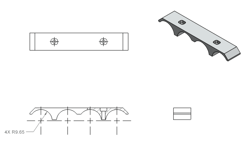
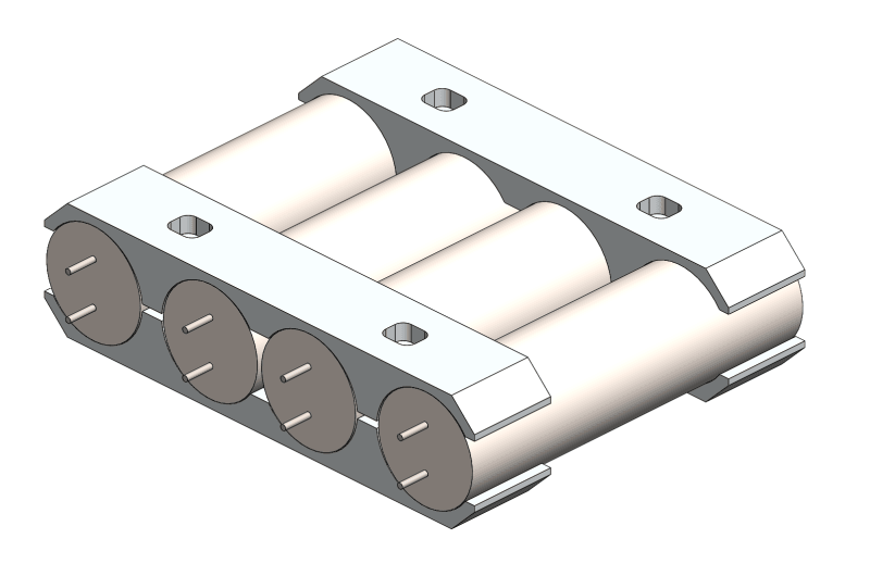
I'm mainly concerned with controlling the positions of the cells relative to each other and making sure they are parallel, so that the leads can be inserted into a mating PCB without excessive stress. Perpendicularity between the cells and the end of the clamp is secondary, and the rest of the profile that is not in contact with the cells does not need to be tightly controlled.

Can anyone recommend an appropriate set of datums for this? I don't use GD&T often, so I'm a bit out of my depth here.
 
Replies continue below

Recommended for you

The problem statement is a bit off. The real problem is to provide a pressure on the cells that won't tend to crease or dent the cells.

One way to deal with this is to have the a close fit - applying a profile of surface tolerance to each of the contacting surfaces would be a start. I would match the maximum diameter of the cells and have a tolerance that only allowed that to increase by a small margin.

However, the plastic won't automatically conform if the radius is larger in the part than of the cell and variation in cell diameter can cause problems as it will squeeze only on a high spot. I am not sure that this clamp method is typical for cells like this. I would think a restraint on the cap end and a base plate with a spring to keep the cell from moving would be better.

How does this compare with existing products?
 
A bit more consideration - I have seen where the cells are given a largish gap, then soldered to the circuit board and then the gap is filled with hot-melt glue. This avoids the need for precision and the possibility of straining the connect. Such a glue operation is often used on circuit boards to secure capacitors and other tall components.
 
Hi Dave,

I didn't want to get too far into the details in my original post since this is mostly a GD&T question, but this is based on a design that we have previously vibe tested and flown (CubeSat battery). However, in that design only two cells were clamped together instead of four.

The clamps are 6061, not plastic, and the cells are wrapped in Kapton tape.

I would match the maximum diameter of the cells and have a tolerance that only allowed that to increase by a small margin.

This is the approach I used in the previous version - the cells with tape are around 18.6 mm diameter (R9.3), while the radius of the clamp is 9.65 (or slightly larger).

The real problem is to provide a pressure on the cells that won't tend to crease or dent the cells.
The plastic won't automatically conform if the radius is larger in the part than of the cell and variation in cell diameter can cause problems as it will squeeze only on a high spot.

We flew the previous version with very low preload on the fasteners. With the low preload and contact only at the high spots, we didn't experience any damage to the cells or slippage between cells and clamp. Even when applying a large load axially to the end of the cells, they didn't slip. Admittedly, this four-cell version is different, since we're now relying on a combination of uniformly sized cells and flexibility of the 6061 part. If, for example, we have three large cells and one small one, the small one might slip. If that happens, I figure I'll just add more tape to the small cells.

Regarding strain on the leads, there is a large gap between the cells and the PCB, and the leads aren't soldered - they use pin receptacles. This does provide quite a bit of misalignment tolerance.

I'm confident that the design will work, either as is or with extra tape on the cells.

I'm just not sure where to place the datums. I'm hesitant to use any of the flat surfaces, since none of them are critical to the assembly. Can I use the axis of one of the mating surfaces as the primary datum? I also want to avoid any ambiguity, since the part is symmetric.
 
As mentioned before - One way to deal with this is to have the a close fit - applying a profile of surface tolerance to each of the contacting surfaces would be a start. I would match the maximum diameter of the cells and have a tolerance that only allowed that to increase by a small margin.

Is this not bolted in place to a structure intermediate between the cells and the circuit board? That interface between one clamp and the intermediate structure should be a primary reference. You can use both features as the datum references for all other faces depending on the simultaneous requirements if used with profile of surface tolerances
 
I would use the large flat top surface as Datum A, the long surface that is perpendicular to that and that is flush with the end of the cells as Datum B, and the overall length dimension which touches off the the short ends as Datum C because this part is symmetrical. Then use a profile control on the curved pockets.
 
How does this look?

surface_datums_ufqfvf.png


How about if the two ends are curved, rather than parallel surfaces - something like this:

curved_cmqmz0.png


Is datum C still valid if the overall width is an irregular feature of size?
 
Hi, itar:

Did you ever see how CMM programmer run a CMM machine? Your CMM programmer uses a fixture to place your part against datum feature A, and slide to datum feature B. Then he or she will push the part against a stopper with either left side or right feature. Datum C will be established in the program in addition to datum A and B.

Best regards,

Alex
 
It can be an ad hoc fixture from bolting some precision angle blocks to the inspection table. Place the part with the flat side on the table, place the side surface against one precision angle block and slide the part to contact the second, likely smaller one. Finally, slide a gauge block against the other short side and indicate on the table, the larger angle block, and then on both the smaller angle block and the gauge block to figure the center point. The gauge block needs to be firm against both the table and the large angle block to pick up the highest point on the part while remaining parallel to the face of the opposing angle block.

So, three taps on the table, two on the big angle block, and one each on the small angle block and the gauge block.

Then it is off to the races for the grooves and tippy-tapping as many points as will make the inspector happy that the surface coordinates are enough to catch all the variation. Also, picking up the two holes. Getting the recesses will be more of a challenge unless their primary is individually the holes they are tied to.
 
Itar,
When the part will be inspected per your drawing from 12 Jun 24 06:18,
How will the inspecor know which side is datum feature A on the physical part?
Is there any preference to the side face selected as datum feature A over the opposite one?
 
It isn't required for the inspector to know that. If the part fails in one orientation, the inspector flips it over and if it passes in the second orientation the part is acceptable. While it may increase inspection time, it will also tend to cut scrap rates as either side as the datum feature could be acceptable or, if only one is, then that's enough.

The person who may need to know is the installer.

Burunduk, do you see in the application proposed a problem for the installation if a non-contacting surfaces are oriented one way or the other?

However, I would not make that face the primary datum feature. It is small and, when used as the lower clamp part, doesn't contact the mounting surface. The large flat surface should be the primary datum feature as it does make contact with and is responsible for orienting the part against the mating surface where it is assembled.
 
3D, it looks like you missed the part of the training that says not to prioritize one side of a width for datum selection if both sides serve the same function. Especially when they are indistinguishable. But your assumption that both sides have equal importance is also incorrect. Those surfaces clearly face different neighbors in the assembly, and one will have less clearance to nearby components.
 
I'm sure this will start a holy war....

It's often taught that
Datum Features are real, tangible features on a part where the measurement equipment would physically touch or measure.  They are usually important functional surfaces.

The currently proposed datum features A B C seem to all have zero functional relevance to this part.
 
It looks like you are trying to align parts with screws. Could you use hollow dowel pins for alignment then use a touch smaller screw to fasten the two parts together. You then could use these dowel pins holes/ slots as your datum features, and they should be able to be held really tight with FOS and position, giving you a great alignment option between the two parts. You could also use alignment tabs or design some extra features you could machine to help keep these parts aligned like you want. How are these parts manufactured, what procees?
 
MJ - to the extent the mounting problem is defined so far, I agree, which is why I wrote:

Is this not bolted in place to a structure intermediate between the cells and the circuit board? That interface between one clamp and the intermediate structure should be a primary reference. You can use both features [that interface and the slots] as the datum references for all other faces depending on the simultaneous requirements if used with profile of surface tolerances

If it isn't attached to any intermediate structure, which would be really unusual for something derived from a CubeSat installation, then my original suggestion:

applying a profile of surface tolerance to each of the contacting surfaces would be a start

A continuation would have been to used those contacting surfaces as the primary datum feature for profile/position tolerances and depend on simultaneous requirements to located those remaining surfaces to one another, but then no more installation details were forthcoming.
 
B,

But your assumption that both sides have equal importance is also incorrect. Those surfaces clearly face different neighbors in the assembly, and one will have less clearance to nearby components.

"The person who may need to know is the installer."

You are always incorrect when you speculate about assumptions, particularly when I didn't make any. The installer may need to know, or the tolerance stack may be such that it doesn't matter which way the part goes in relative to the way the part was inspected.

The easiest cure, if one is required, is to either add a feature or mark to make the part distinguishable for the installer and the inspector.

One might also add another datum feature symbol to mark the other side as a datum feature and then add another FCF to use that in place of the front one so that the related features are inspected in both DRFs. This has the advantage that no orientation feature is required and the installer cannot put the part in the wrong way.

Certainly this comes up in the training you perform or attend, but you chose not to suggest one, choosing sniping instead.
 
Status
Not open for further replies.
Back
Top