Eng-Tips is the largest engineering community on the Internet

Intelligent Work Forums for Engineering Professionals

Some symbol help please 1

Status
Not open for further replies.

itsmoked

Electrical
Feb 18, 2005
19,114
0
0
US
FETs_rlkhjw.png


The original designer has passed so I'm having to reverse engineer this whole thing. It's got a lot of these two types of symbols.

What are Q9 and Q10??

Keith Cress
kcress -
 
Replies continue below

Recommended for you

They're MOSFETs. Presumably, one is an n-channel and the other is a p-channel; Q9 is supposedly n-channel and Q10 is p-channel, based on
[edit]btw, that symbol collection is ANCIENT; the date of the book is only about 3 years after when the first MOSFET-based ICs came out.

circuit-symbol-transistor-mosfet-enhancement-02.gif


TTFN (ta ta for now)
I can do absolutely anything. I'm an expert! faq731-376 forum1529 Entire Forum list
 
Agree. MOSFET:s created lots of confusion when they were introduced some 50 years ago. Many different symbols and, to add insult to injury, there were also enrichment and depletion types, which wasn't obvious from the symbols. And still isn't. Do you have any type numbers? There are old data books on some of the early devices.


Gunnar Englund
--------------------------------------
Half full - Half empty? I don't mind. It's what in it that counts.
 
Yeah, old as dirt Mike. LOL
I gave it a long look but also didn't find anything close.


IR; I think those symbols are mis-marked! Notice the arrow directions compared to these two symbols I just cut out of data sheets.

P-Channel_ufwzao.png


N-Channel_x5iwlf.png


The author of the schematic was a bit eclectic stuffing more than 200 parts, including 15 ICs, on a single 8-1/2x11 page leaving lots of details out, like part numbers of these devices, and the whole shebang is controlled by an FPGA and it's only presence in the schematic is some round circles with pin numbers.
qp2kcm.gif


Thanks for the discussion.

Keith Cress
kcress -
 
I think that a black box approach would be better than reverse-engineering.

Have the customer describe what that thing is supposed to do. It is usually possible to create better functionality with a little MCU plus some discrete components. And also throw in a few improvements that they (perhaps) have been wanting all their life.

Gunnar Englund
--------------------------------------
Half full - Half empty? I don't mind. It's what in it that counts.
 
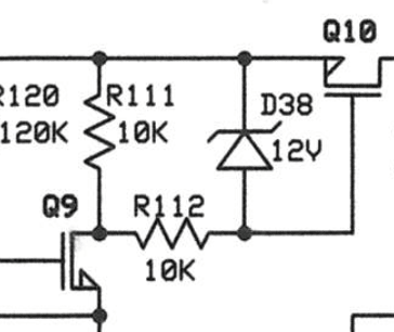
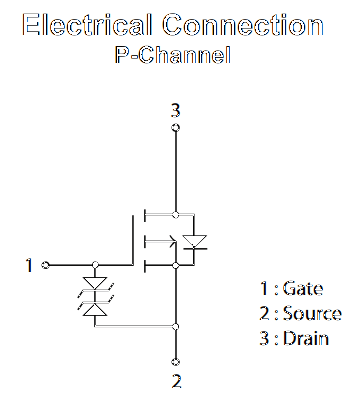
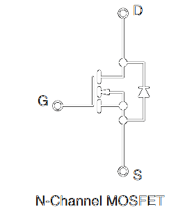
As some articles point out, your original set of symbols are different than the ones that specify the body diodes, which are relative to the channel, hence, they point to the middle of the gate region. These, I think, are supposed to indicate the source terminal and direction of conventional current, hence ">" indicates a transistor where conventional current flows out of the source, making it n-channel, while the other device has conventional current flowing into the source, making p-channel. Moreover, the structure of the circuit suggests that the gate-source of Q10 is controlled by the common-source Q9, and the only way to shut off Q10 would be if Q10 is p-channel. Slight bias confirmation on my part, possibly.

{edit] I think this set of symbols is more consistent with BJT symbology. which likewise shows conventional current direction at the emitter. The body diode symbology was always an extra step for cognitive processing to say, "p-type" body, so "n-type" channel, so n-channel. BJT symbology, arrow points out --> NPN

TTFN (ta ta for now)
I can do absolutely anything. I'm an expert! faq731-376 forum1529 Entire Forum list
 
Gunnar; I probably used the wrong term as I know exactly what it does and they are happy to tell me anything I ask them. It's just that they've been building these things for 10 years off of a hand doctored not fully complete schematic. They want it turned into a smaller version with newer SMD parts instead of strictly thru-hole parts about to get obsoleted. I'd love to do it with a micro - trivial! Massive performance improvement. Easy feature additions. Alas it's for aviation and I'm told replacing the FPGA with a micro would be a quarter-million dollar testing tragedy.


IR; I've always used the NPN (Not Pointing iN) heuristic tool. Doesn't work for FETs as it's backwards..
I'm looking at the schematic to suss out the parts. I also have a unit so I can look at the parts and hunt down data sheets. Unfortunately it's at my office and I'm stuck in the house with a long running flu.


Keith Cress
kcress -
 
I like your wording, Keith. "Tragedies" should be avoided.
I'm right now about to enter a similar situation. Perhaps I should stay out. But there's an interesting financial aspect in it, too. And a technical challenge. Or several.

Gunnar Englund
--------------------------------------
Half full - Half empty? I don't mind. It's what in it that counts.
 
Non-pointing-in doesn't work on the convention MOS symbol, because the arrow refers to the body diode. In your schematic, it should work, because the arrow is comparable to the emitter arrow on an NPN, and not referring to the body diode. The body diode is almost moot in most modern monolithic MOSFETs, because the body is often already shorted to the source. The body connection only made sense in multi-transistor ICs, because n-channel transistors running in a cascode or as a pullup would have their body junctions still at ground, resulting in a substantial increase in threshold voltage, compared to a ground source device. But, that sort of thing has mostly gone by the wayside since CMOS ICs became the norm.

Gunnar made reference to depletion-mode transistors, which were used in NMOS-only ICs as substitutes for high-value load resistors. They were the bulk of the devices affected by body effect threshold shifts.

TTFN (ta ta for now)
I can do absolutely anything. I'm an expert! faq731-376 forum1529 Entire Forum list
 
KC said:
I'm looking at the schematic to suss out the parts. I also have a unit so I can look at the parts and hunt down data sheets. Unfortunately it's at my office and I'm stuck in the house with a long running flu.

There should also be a Parts List somewhere. Perhaps the client can email you a copy of it.

 
The only interpretation leading to working and reasonable circuit is as follows: Q9 N-channel-Mosfet, Q10 P-channel-Mosfet

There is no need to worry about the symbols, polarity and voltage of the Z-diode allows to draw this conclusion
 
Status
Not open for further replies.
Back
Top